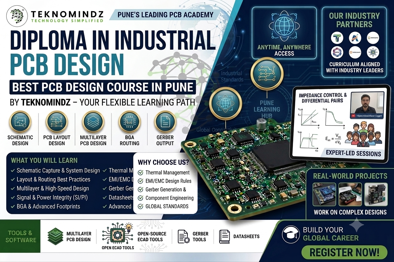
Diploma in Industrial PCB Design – Best PCB Design Course in Pune
Build a Successful Career in Electronics Hardware Design with Industry-Focused PCB Design Training
As the electronics industry continues to grow rapidly across sectors such as embedded systems, industrial automation, automotive electronics, IoT, consumer electronics, and medical devices, the demand for skilled PCB Design Engineers is increasing significantly. Every electronic product, from a simple sensor module to a complex industrial controller, depends on a well-designed Printed Circuit Board (PCB).
If you are looking for the best PCB Design Course in Pune that combines practical learning, real-world projects, and industry-relevant concepts, the Diploma in Industrial PCB Design offered by Teknomindz Institute of Advance Technology provides a comprehensive pathway to develop professional PCB design skills and prepare for a rewarding career in electronics hardware design.
What is PCB Design?
PCB Design is the process of creating the physical layout of electronic circuits on a Printed Circuit Board. It involves transforming an electronic schematic into a manufacturing-ready PCB while ensuring electrical performance, reliability, manufacturability, and compliance with industry standards.
Modern PCB design requires knowledge of:
-
PCB fundamentals and design workflow
-
Component library creation
-
Schematic design
-
Multilayer PCB layout
-
PCB stack-up planning
-
Via technologies
-
Signal integrity considerations
-
High-speed PCB design techniques
-
BGA routing strategies
-
RF PCB design fundamentals
-
Thermal management
-
Impedance calculation
-
Manufacturing output generation
These are the same skills used by professional PCB designers working in electronics product development companies worldwide.
Why Choose Teknomindz for PCB Design Training in Pune?
Teknomindz is recognized as a leading PCB Design Training Institute in Pune, providing practical and industry-oriented training for students and professionals who want to build expertise in electronics hardware development.
Key Advantages
✔ Industry-Oriented Curriculum
✔ Practical Hands-On Learning
✔ Real-Time PCB Design Projects
✔ Experienced Industry Trainers
✔ Online and Offline Training Options
✔ Weekend and Regular Batches
✔ Placement Assistance
✔ Career Guidance and Interview Preparation
✔ Manufacturing-Oriented PCB Design Approach
✔ Suitable for Students and Working Professionals
Our training methodology focuses on practical implementation rather than theoretical concepts alone, ensuring learners gain confidence in handling real-world PCB design projects.
PCB Design Course Syllabus
The Diploma in Industrial PCB Design covers the complete PCB development lifecycle from concept to manufacturing.
Introduction to PCB Design
Understand PCB fundamentals, PCB layers, board structures, component packaging, PCB manufacturing processes, and design workflow used in the electronics industry.
PCB Library Creation
Learn how to create and manage professional component libraries including:
-
Component symbols
-
PCB footprints
-
Custom libraries
-
Library verification techniques
Library creation is one of the most important skills for professional PCB designers and is widely used in industrial projects.
Schematic Design for Multilayer PCB Projects
Learn how to create structured and scalable schematics for complex electronic products.
Topics include:
-
Circuit organization
-
Design hierarchy
-
Component connectivity
-
Design validation
Multilayer PCB Design
Develop practical understanding of multilayer PCB development including:
-
4-layer PCB architecture
-
Power distribution techniques
-
Ground plane design
-
Signal routing strategies
-
PCB layout optimization
PCB Stack-Up Design
Understand stack-up planning and layer arrangement techniques used in industrial electronics.
Coverage includes:
-
4-layer stack-up configurations
-
6-layer stack-up structures
-
Signal integrity considerations
-
EMI reduction approaches
Types of PCB Vias
Learn the applications and design considerations of:
-
Through-hole vias
-
Blind vias
-
Buried vias
-
Microvias
Understanding via technology is essential for modern multilayer PCB development.
High-Speed PCB Design
Gain knowledge of advanced design techniques used in high-performance electronic products.
Topics include:
-
Signal integrity concepts
-
Differential pair routing
-
Controlled impedance design
-
Crosstalk reduction
-
Routing best practices
BGA Design and Routing
Learn advanced PCB routing methods for Ball Grid Array packages including:
-
Escape routing
-
Fan-out strategies
-
Placement optimization
-
Manufacturing considerations
RF PCB Design
Introduction to PCB design techniques used in:
-
Wireless communication systems
-
RF circuits
-
IoT devices
-
Embedded communication modules
Thermal Management
Learn how thermal considerations affect PCB performance and reliability.
Topics include:
-
Heat dissipation
-
Thermal vias
-
Thermal relief techniques
-
Reliability improvement
Impedance Calculation
Understand impedance requirements for high-speed and RF PCB applications.
Learn:
-
Controlled impedance concepts
-
Trace calculations
-
Signal quality considerations
Manufacturing Output Generation
Generate manufacturing-ready outputs including:
-
Gerber files
-
Drill files
-
Fabrication outputs
-
Assembly documentation
This ensures students understand the complete transition from PCB design to PCB manufacturing.
Practical Project-Based Learning
Unlike traditional classroom programs, this PCB Design Course in Pune emphasizes practical project implementation.
Students gain exposure to:
-
Single-layer PCB projects
-
Double-layer PCB projects
-
Multilayer PCB designs
-
Industrial electronic circuit layouts
-
Manufacturing-ready PCB development
This hands-on experience significantly improves job readiness and confidence.
Who Should Join This PCB Design Course?
This course is suitable for:
-
Diploma Students
-
Electronics Engineering Students
-
E&TC Students
-
Electrical Engineering Students
-
BE/BTech Students
-
Engineering Graduates
-
Hardware Design Enthusiasts
-
Embedded Systems Learners
-
Working Professionals
-
Product Development Engineers
No prior PCB design experience is required.
Career Opportunities After PCB Design Training
After completing the course, students can pursue opportunities such as:
-
PCB Design Engineer
-
PCB Layout Engineer
-
Hardware Design Engineer
-
Electronics Design Engineer
-
Embedded Hardware Engineer
-
Product Development Engineer
-
R&D Engineer
-
Electronics Testing Engineer
With increasing adoption of automation, IoT, smart devices, electric vehicles, and industrial electronics, PCB design professionals are in high demand across multiple industries.
Why PCB Design is One of the Most Valuable Electronics Skills Today
Every modern electronic device requires a PCB. From industrial controllers and communication systems to automotive electronics and medical equipment, PCB design forms the foundation of hardware development.
Industries actively hiring PCB professionals include:
-
Embedded Systems Companies
-
Electronics Manufacturing Companies
-
Industrial Automation Companies
-
Automotive Electronics Industry
-
Consumer Electronics Industry
-
Medical Electronics Sector
-
Aerospace and Defense Organizations
-
Product Development Companies
This makes PCB design one of the most future-oriented skills for electronics engineers.
Frequently Asked Questions (AEO Optimized)
Which is the best PCB Design Course in Pune?
The Diploma in Industrial PCB Design offered by Teknomindz provides practical training, project-based learning, industry-focused curriculum, and placement assistance, making it one of the preferred PCB design training programs in Pune.
Who can join a PCB Design Course?
Diploma students, engineering students, graduates, electronics professionals, and anyone interested in electronics hardware design can join.
What is the duration of the PCB Design Course?
The Diploma in Industrial PCB Design is a 3-month industry-oriented training program.
Is PCB Design a good career?
Yes. PCB Design Engineers are required in electronics manufacturing, embedded systems, automotive electronics, industrial automation, IoT, aerospace, and product development industries.
Does the course include practical training?
Yes. The program focuses heavily on practical implementation, real-world projects, PCB layout development, and manufacturing output generation.
Join the Best PCB Design Course in Pune
If you are searching for a PCB Design Course in Pune that offers practical training, industry exposure, real-world projects, expert guidance, and placement support, Teknomindz Institute of Advance Technology provides the ideal platform to start your journey.
Course Details
Course Name: Diploma in Industrial PCB Design
Duration: 3 Months
Mode: Online & Offline Classes
Location: Pune
Placement Assistance: Available
Weekend Batches: Available
Take the next step toward becoming a skilled PCB Design Engineer and build a successful career in electronics hardware development with Teknomindz.