
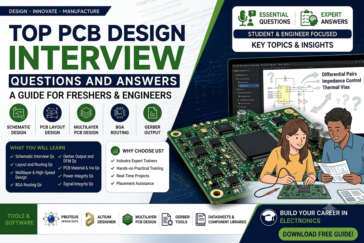
Top PCB Design Interview Questions and Answers for Freshers & Engineers in Pune
If you are preparing for a career in electronics hardware design, embedded systems, or product development, understanding common PCB design interview questions can significantly improve your chances of success. Companies hiring PCB Design Engineers, Hardware Design Engineers, Embedded Hardware Engineers, and Electronics Design Engineers often assess candidates on PCB fundamentals, multilayer design concepts, manufacturing processes, signal integrity, and industry-standard tools.
This guide covers the most frequently asked PCB Design Interview Questions and Answers for students pursuing a PCB Design Course in Pune and professionals looking to enter the electronics industry.
1. What is a PCB?
A Printed Circuit Board (PCB) is a board used to mechanically support and electrically connect electronic components through conductive copper tracks, pads, and vias.
PCBs are used in:
- Embedded Systems
- Consumer Electronics
- Industrial Automation
- Medical Devices
- Automotive Electronics
- IoT Products
2. What are the main stages of PCB Design?
Typical PCB Design Flow:
- Requirement Analysis
- Schematic Design
- Component Selection
- Library Creation
- PCB Layout Design
- Routing
- Design Rule Check (DRC)
- Gerber Generation
- Manufacturing
- Testing & Validation
3. What is the difference between Schematic Design and PCB Layout?
Schematic Design
Represents logical electrical connections between components.
PCB Layout
Represents the physical placement and routing of components on the PCB.
4. What are PCB Layers?
PCB layers are copper layers used for signal routing, power distribution, and grounding.
Examples:
- Single Layer PCB
- Double Layer PCB
- 4 Layer PCB
- 6 Layer PCB
- 8 Layer PCB
5. Why are Multilayer PCBs used?
Advantages:
- Higher Component Density
- Better Signal Integrity
- Reduced EMI
- Dedicated Power and Ground Planes
- Compact Design
6. What is a Via?
A via is a conductive hole used to connect different PCB layers.
Types include:
- Through Hole Via
- Blind Via
- Buried Via
- Micro Via
7. What is the difference between Blind Via and Buried Via?
Blind Via
Connects an outer layer to an inner layer.
Buried Via
Connects only inner layers and is not visible externally.
8. What is PCB Stack-Up?
PCB stack-up defines the arrangement of copper and dielectric layers.
Example:
- Signal Layer
- Ground Plane
- Power Plane
- Signal Layer
Proper stack-up improves signal integrity and EMI performance.
9. What is Signal Integrity?
Signal Integrity refers to maintaining signal quality during transmission through PCB traces.
Problems include:
- Reflection
- Crosstalk
- Noise
- Distortion
10. What is Crosstalk?
Crosstalk occurs when signals from one trace interfere with nearby traces due to electromagnetic coupling.
Prevention methods:
- Increase spacing
- Use Ground Planes
- Proper Routing
11. What is Controlled Impedance?
Controlled impedance ensures PCB traces maintain a specific impedance value for high-speed signal transmission.
Used in:
- USB
- HDMI
- Ethernet
- DDR Memory Interfaces
12. What is Differential Pair Routing?
Two traces carrying equal and opposite signals.
Examples:
- USB
- CAN
- Ethernet
- LVDS
Benefits:
- Noise Immunity
- Better Signal Integrity
13. What is Ground Plane?
A continuous copper layer connected to ground.
Benefits:
- Noise Reduction
- Better Return Path
- EMI Reduction
14. What is a Power Plane?
A dedicated layer used for power distribution.
Advantages:
- Stable Voltage Distribution
- Reduced Voltage Drops
15. What is DRC?
Design Rule Check verifies that PCB design follows manufacturing rules.
Checks:
- Trace Width
- Clearance
- Pad Sizes
- Via Sizes
16. What is ERC?
Electrical Rule Check validates schematic connections.
Detects:
- Missing Connections
- Incorrect Nets
- Electrical Violations
17. What is PCB Footprint?
Physical representation of a component on the PCB.
Includes:
- Pads
- Silkscreen
- Courtyard
- Assembly Information
18. What is a PCB Library?
Collection of:
- Symbols
- Footprints
- Component Models
Used for schematic and PCB design.
19. What is BGA?
BGA (Ball Grid Array) is a package where solder balls are arranged underneath the IC.
Advantages:
- High Pin Count
- Compact Size
- Better Thermal Performance
20. What is Fan-Out in BGA Routing?
The process of routing signals from BGA pads to accessible PCB traces.
21. Why is Thermal Management Important?
Proper thermal management:
- Improves Reliability
- Prevents Overheating
- Extends Product Life
Methods:
- Thermal Vias
- Heat Sinks
- Copper Pours
22. What are Thermal Vias?
Vias placed beneath hot components to transfer heat to other PCB layers.
23. What is EMI?
Electromagnetic Interference generated by electronic circuits.
Can affect:
- Signal Quality
- Device Performance
24. What is EMC?
Electromagnetic Compatibility refers to a product's ability to operate without causing or receiving interference.
25. What are Gerber Files?
Industry-standard files used for PCB manufacturing.
Contain:
- Copper Layers
- Solder Mask
- Silkscreen
- Board Outline
26. What is NC Drill File?
Contains drill hole information used during PCB fabrication.
27. What is PCB Routing?
The process of creating copper traces between components.
28. What is Copper Pour?
A large copper-filled area used for:
- Grounding
- Power Distribution
- Heat Dissipation
29. What is Trace Width?
Width of copper tracks used for signal and power transmission.
Depends on:
- Current Capacity
- Voltage
- Temperature Rise
30. What Happens if Trace Width is Too Small?
- Excessive Heating
- Voltage Drop
- PCB Failure
31. What is Design for Manufacturing (DFM)?
DFM ensures the PCB can be manufactured reliably and cost-effectively.
32. What is Design for Assembly (DFA)?
DFA focuses on ease of PCB assembly and production.
33. What PCB Design Software Have You Used?
Common answers:
- Altium Designer
- Proteus
- KiCad
- Eagle
- OrCAD
34. Why Do Companies Prefer Altium Designer?
- Advanced Routing Tools
- 3D Visualization
- Industry Acceptance
- Better Library Management
35. What Are High-Speed PCB Design Challenges?
- Signal Integrity
- Impedance Control
- Crosstalk
- EMI
- Timing Issues
36. How Do You Reduce Noise in PCB Design?
Methods include:
- Proper Grounding
- Ground Planes
- Decoupling Capacitors
- Controlled Routing
37. What is a Decoupling Capacitor?
Capacitor placed near IC power pins to filter voltage fluctuations.
38. What Are Design Constraints?
Rules applied during PCB design such as:
- Trace Width
- Clearance
- Differential Pair Rules
- Length Matching
39. What Is Length Matching?
Ensuring critical signals travel equal distances.
Commonly used in:
- DDR Memory
- High-Speed Interfaces
40. Why Do You Want a Career in PCB Design?
Sample Answer:
"PCB Design combines electronics knowledge with practical product development. I enjoy working on hardware design and creating real-world electronic products. Through my PCB Design Course in Pune, I have gained experience in schematic design, multilayer PCB layout, Altium Designer, and manufacturing processes, which motivates me to build a career in hardware design."
Final Interview Preparation Tips
Before attending a PCB Design interview:
✔ Understand PCB Design Flow
✔ Practice Altium Designer & Proteus
✔ Learn Gerber Generation
✔ Understand Multilayer PCB Design
✔ Study Signal Integrity Basics
✔ Revise Vias, Stack-Up & Ground Planes
✔ Build Small PCB Projects
✔ Review Manufacturing Processes
A strong understanding of these topics will help you confidently answer PCB Design interview questions and improve your chances of securing a role as a PCB Design Engineer, Hardware Design Engineer, or Embedded Hardware Engineer.